logistic_guy
Senior Member
- Joined
- Apr 17, 2024
- Messages
- 1,610
here is the question
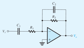
Derive the transfer function for the operational amplifier (an ideal op amp) in the figure and show that it can be written in the form ViVo=[1+(ω1/jω)][1+(ω/ω2)]−R2/R1 where ω1=C1R11 and ω2=C2R21. Assuming that the circuit is designed such that ω2≫ω1, find approximate expressions for the transfer function in the following frequency regions:
(a) ω≪ω1
(b) ω1≪ω≪ω2
(c) ω≫ω2
Use these approximations to sketch a Bode plot for the magnitude response. Observe that the circuit performs as an amplifier whose gain rolls off at the low-frequency end in the manner of a high-pass STC network, and at the high-frequency end in the manner of a low-pass STC network. Design the circuit to provide a gain of 40 dB in the “middle-frequency range,” a low-frequency 3-dB point at 200 Hz, a high-frequency 3-dB point at 200 kHz, and an input resistance (at ω≫ω1) of 2 kΩ.

my attemb
according to this website
 masteringelectronicsdesign.com
the transfer function for the inverting amplifier is Vo=−ViR1R2 which can be written as ViVo=−R1R2
but the circuit in the website don't have capacitors C1 and C2
what should i do in this case?
Derive the transfer function for the operational amplifier (an ideal op amp) in the figure and show that it can be written in the form ViVo=[1+(ω1/jω)][1+(ω/ω2)]−R2/R1 where ω1=C1R11 and ω2=C2R21. Assuming that the circuit is designed such that ω2≫ω1, find approximate expressions for the transfer function in the following frequency regions:
(a) ω≪ω1
(b) ω1≪ω≪ω2
(c) ω≫ω2
Use these approximations to sketch a Bode plot for the magnitude response. Observe that the circuit performs as an amplifier whose gain rolls off at the low-frequency end in the manner of a high-pass STC network, and at the high-frequency end in the manner of a low-pass STC network. Design the circuit to provide a gain of 40 dB in the “middle-frequency range,” a low-frequency 3-dB point at 200 Hz, a high-frequency 3-dB point at 200 kHz, and an input resistance (at ω≫ω1) of 2 kΩ.

my attemb
according to this website
How to Derive the Inverting Amplifier Transfer Function – Mastering Electronics Design
the transfer function for the inverting amplifier is Vo=−ViR1R2 which can be written as ViVo=−R1R2
but the circuit in the website don't have capacitors C1 and C2
what should i do in this case?
